
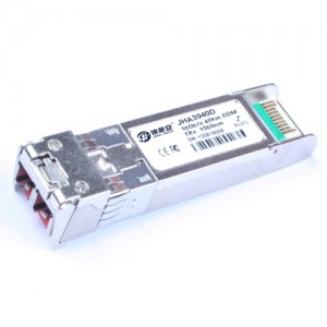
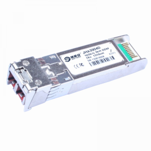
10Gb/s 20km BiDi SFP+ Transceiver, 1270nm/1330nm CWDM, JHA5920D-2733&3327

Features:
*Supports 9.95Gb/s to 11.3Gb/s bit rates
*Hot-pluggable SFP+ footprint
* Single LC for Bi-directional Transmission
* Maximum link length of 20km
* Built-in 1270/1330 WDM Filter
* Uncooled 1270nm or 1330nm CWDM DFB Laser.
* Power dissipation <1.5W
* No Reference Clock required
* Built-in digital diagnostic functions
* Temperature range 0°C to 70°C
* Very low EMI and excellent ESD protection
* RoHS Compliant Part
Applications:
* 10GBASE-LR/LW Ethernet
* SONET OC-192 / SDH
* 10G Fibre Channel
Description:
JHA5920D-2733 & JHA5920D-3327 Bi-directional 10Gb/s (SFP+) transceivers are compliant with the current SFP+ Multi-Source Agreement (MSA) Specification. They comply with 10GBASE-LR/LW Ethernet, SONET OC-192 / SDH and 10G Fibre Channel 1200-SM-LL-L. Digital diagnostics functions are available via a 2-wire serial interface, as specified in the SFP+ MSA.
l Absolute Maximum Ratings
|
Parameter |
Symbol |
Min. |
Typical |
Max. |
Unit |
| Storage Temperature |
TS |
-40 |
|
+85 |
°C |
| Supply Voltage |
VCCT, R |
-0.5 |
|
4 |
V |
| Relative Humidity |
RH |
0 |
|
85 |
% |
l Recommended Operating Environment
|
Parameter |
Symbol |
Min. |
Typical |
Max. |
Unit |
| Case operating Temperature |
TC |
-5 |
|
+70 |
°C |
| Supply Voltage |
VCCT, R |
+3.135 |
|
+3.465 |
V |
| Supply Current |
ICC |
|
|
450 |
mA |
| Power Dissipation |
PD |
|
|
1.5 |
W |
l Electrical Characteristics (TOP = 0 to 70 °C, VCC = 3.135 to 3.465 Volts)
|
Parameter |
Symbol |
Min |
Typ |
Max |
Unit |
Note |
||
| Transmitter: | ||||||||
| Differential input voltage swing |
|
180 |
|
700 |
mVpp |
1 |
||
| Transmit Disable Input | H |
VIH |
2.0 |
|
Vcc+0.3 |
V |
|
|
| L |
VIL |
0 |
|
0.8 |
V |
|
||
| Transmit Enable Output | H |
VOH |
2.4 |
|
Vcc+0.3 |
V |
|
|
| L |
VOL |
0 |
|
0.4 |
V |
2 |
||
| Input Differential Impedance |
Zin |
80 |
100 |
120 |
Ω |
|
||
| Receiver | ||||||||
| Differential output voltage swing |
|
300 |
|
850 |
mVpp |
3 |
||
| LOS Output | H |
VOH |
2.4 |
|
Vcc+0.3 |
V |
2 |
|
| L |
VOL |
0 |
|
0.4 |
V |
|
||
| Output Differential Impedance |
Zon |
80 |
100 |
120 |
Ω |
|
||
Notes:
Note 1) TD+/- are internally AC coupled with 100Ω differential termination inside the module.
Note 2) Tx Fault and Rx LOS are open collector outputs, which should be pulled up with 4.7k to 10kΩ resistors on the host board. Pull up voltage between 2.0V and Vcc+0.3V.
Note 3) RD+/- outputs are internally AC coupled, and should be terminated with 100Ω (differential) at the user SERDES.
l Optical Parameters(TOP = 0 to 70°C, VCC = 3.135 to 3.465 Volts)
|
Parameter |
Symbol |
Min |
Typ |
Max |
Unit |
Ref. |
||
| Transmitter | ||||||||
| Bit Rate |
BR |
9.9 |
|
11.3 |
Gb/s |
|
||
| Optical Wavelength | JHA5920D-2733 |
λ |
1260 |
1270 |
1280 |
nm |
|
|
| JHA5920D-3327 |
|
1320 |
1330 |
1340 |
|
|||
| Average output power |
Po |
-3 |
|
+2 |
dBm |
|
||
| Optical Extinction Ratio |
ER |
3.5 |
|
|
dB |
|
||
| Spectral width |
Δλ |
|
|
1 |
nm |
|
||
| Side Mode Suppression Ratio |
SMSR |
30 |
|
|
dB |
|
||
| Optical Eye Mask |
|
Compliant with IEEE802.3ae |
|
|||||
| Receiver | ||||||||
| Bit Rate |
BR |
9.9 |
|
11.3 |
Gb/s |
|
||
| Optical Wavelength | JHA5920D-2733 |
λ |
1320 |
1330 |
1340 |
nm |
|
|
| JHA5920D-3327 |
|
1260 |
1270 |
1280 |
|
|
||
| Receiver Sensitivity |
Sen |
|
|
-14.5 |
dBm |
1 |
||
| Maximum Input Power |
PMAX |
0 |
|
|
dBm |
|
||
| LOS De-Assert |
LOSD |
|
|
-15 |
dBm |
|
||
| LOS Assert |
LOSA |
-25 |
|
|
dBm |
|
||
| LOS Hysteresis |
LOSH |
0.5 |
|
4 |
dB |
|
||
Notes:
Note 1) Measured with a PRBS of 231-1 at 1 x 10-12 BER and 3.5 dB extinction ratio.
l Pin Assignment
Diagram of Host Board Connector Block Pin Numbers and Name

l Pin Function Definitions
|
PIN # |
Name |
Function |
Notes |
| 1 | VeeT | Module transmitter ground |
1 |
| 2 | Tx Fault | Module transmitter fault |
2 |
| 3 | Tx Disable | Transmitter Disable; Turns off transmitter laser output |
3 |
| 4 | SDL | 2 wire serial interface data input/output (SDA) |
|
| 5 | SCL | 2 wire serial interface clock input (SCL) |
|
| 6 | MOD-ABS | Module Absent, connect to VeeR or VeeT in the module |
2 |
| 7 | RS0 | Rate select0, optionally control SFP+ receiver. When high, input data rate >4.5Gb/s; when low, input data rate <=4.5Gb/s |
|
| 8 | LOS | Receiver Loss of Signal Indication |
4 |
| 9 | RS1 | Rate select0, optionally control SFP+ transmitter. When high, input data rate >4.5Gb/s; when low, input data rate <=4.5Gb/s |
|
| 10 | VeeR | Module receiver ground |
1 |
| 11 | VeeR | Module receiver ground |
1 |
| 12 | RD- | Receiver inverted data out put |
|
| 13 | RD+ | Receiver non-inverted data out put |
|
| 14 | VeeR | Module receiver ground |
1 |
| 15 | VccR | Module receiver 3.3V supply |
|
| 16 | VccT | Module transmitter 3.3V supply |
|
| 17 | VeeT | Module transmitter ground |
1 |
| 18 | TD+ | Transmitter inverted data out put |
|
| 19 | TD- | Transmitter non-inverted data out put |
|
| 20 | VeeT | Module transmitter ground |
1 |
Note 1) The module ground pins shall be isolated from the module case.
Note 2) This pin is an open collector/drain output pin and shall be pulled up with 4.7K-10Kohms to Host_Vcc on the host board.
Note 3) This pin shall be pulled up with 4.7K-10Kohms to VccT in the module.
Note 4) This pin is an open collector/drain output pin and shall be pulled up with 4.7K-10Kohms to Host_Vcc on the host board.
l SFP Module EEPROM Information and Management
The SFP modules implement the 2-wire serial communication protocol as defined in the SFP -8472. The serial ID information of the SFP modules and Digital Diagnostic Monitor parameters can be accessed through the I2C interface at address A0h and A2h. The memory is mapped in Table 1. Detailed ID information (A0h) is listed in Table 2. And the DDM specification at address A2h. For more details of the memory map and byte definitions, please refer to the SFF-8472, “Digital Diagnostic Monitoring Interface for Optical Transceivers”. The DDM parameters have been internally calibrated.
Table 1. Digital Diagnostic Memory Map (Specific Data Field Descriptions)

Table 2 - EEPROM Serial ID Memory Contents (A0h)
|
Data Address |
Length (Byte) |
Name of Length |
Description and Contents |
| Base ID Fields | |||
|
0 |
1 |
Identifier |
Type of Serial transceiver (03h=SFP) |
|
1 |
1 |
Reserved |
Extended identifier of type serial transceiver (04h) |
|
2 |
1 |
Connector |
Code of optical connector type (07=LC) |
|
3-10 |
8 |
Transceiver |
10G Base-LR |
|
11 |
1 |
Encoding |
64B/66B |
|
12 |
1 |
BR, Nominal |
Nominal baud rate, unit of 100Mbps |
|
13-14 |
2 |
Reserved |
(0000h) |
|
15 |
1 |
Length(9um) |
Link length supported for 9/125um fiber, units of 100m |
|
16 |
1 |
Length(50um) |
Link length supported for 50/125um fiber, units of 10m |
|
17 |
1 |
Length(62.5um) |
Link length supported for 62.5/125um fiber, units of 10m |
|
18 |
1 |
Length(Copper) |
Link length supported for copper, units of meters |
|
19 |
1 |
Reserved |
|
|
20-35 |
16 |
Vendor Name |
SFP vendor name: JHA |
|
36 |
1 |
Reserved |
|
|
37-39 |
3 |
Vendor OUI |
SFP transceiver vendor OUI ID |
|
40-55 |
16 |
Vendor PN |
Part Number: “JHA5920D-2733” or “JHA5920D-3327” (ASCII) |
|
56-59 |
4 |
Vendor rev |
Revision level for part number |
|
60-62 |
3 |
Reserved |
|
|
63 |
1 |
CCID |
Least significant byte of sum of data in address 0-62 |
| Extended ID Fields | |||
|
64-65 |
2 |
Option |
Indicates which optical SFP signals are implemented(001Ah = LOS, TX_FAULT, TX_DISABLE all supported) |
|
66 |
1 |
BR, max |
Upper bit rate margin, units of % |
|
67 |
1 |
BR, min |
Lower bit rate margin, units of % |
|
68-83 |
16 |
Vendor SN |
Serial number (ASCII) |
|
84-91 |
8 |
Date code |
JHA’s Manufacturing date code |
|
92-94 |
3 |
Reserved |
|
|
95 |
1 |
CCEX |
Check code for the extended ID Fields (addresses 64 to 94) |
| Vendor Specific ID Fields | |||
|
96-127 |
32 |
Readable |
JHA specific date, read only |
|
128-255 |
128 |
Reserved |
Reserved for SFF-8079 |
l Digital Diagnostic Monitor Characteristics
|
Data Address |
Parameter |
Accuracy |
Unit |
| 96-97 | Transceiver Internal Temperature | ±3.0 | °C |
| 98-99 | VCC3 Internal Supply Voltage | ±3.0 | % |
| 100-101 | Laser Bias Current | ±10 | % |
| 102-103 | Tx Output Power | ±3.0 | dB |
| 104-105 | Rx Input Power | ±3.0 | dB |
l Regulatory Compliance
The JHA5920D-2733 /3327 complies with international Electromagnetic Compatibility (EMC) and international safety requirements and standards (see details in Table following).
| Electrostatic Discharge(ESD) to the Electrical Pins | MIL-STD-883EMethod 3015.7 | Class 1(>1000 V) |
| Electrostatic Discharge (ESD)to the Single LC Receptacle | IEC 61000-4-2GR-1089-CORE | Compatible with standards |
| ElectromagneticInterference (EMI) | FCC Part 15 Class BEN55022 Class B (CISPR 22B)VCCI Class B | Compatible with standards |
| Laser Eye Safety | FDA 21CFR 1040.10 and 1040.11EN60950, EN (IEC) 60825-1,2 | Compatible with Class 1 laserproduct. |
l Regulatory Compliance


Recommended Host Board Power Supply Circuit
Recommended High-speed Interface Circuit
l Mechanical Dimensions

JHA reserves the right to make changes to the products or information contained herein without notice. No liability is assumed as a result of their use or application. No rights under any patent accompany the sale of any such products or information.Published by Shenzhen JHA Technology Co., Ltd.
Copyright © JHA
All Rights Reserved
Products categories
-
10G Single Mode 100Km EML&APD | Dual Fiber...
-
10Gb/s 40km BiDi SFP+ Transceiver, 1270nm/1330n...
-
10G Single Mode 10Km DDM | Dual Fiber SFP+ Tran...
-
10G Multimode 220m FP-LD,1310nm | Dual Fiber SF...
-
10G Single Mode 40Km DDM | Dual Fiber SFP+ Tran...
-
10G Single Mode 2Km FP-LD,1310nm | Dual Fiber S...


