40G QSFP+ SR4, 300m MPO 850nm JHAQC01

Features:
◊ Compliant to the 40GbE XLPPI electrical specification per IEEE 802.3ba-2010
◊ Compliant to QSFP+ SFF-8436 Specification
◊ Aggregate bandwidth of > 40Gbps
◊ Operates at 10.3125 Gbps per electrical channel with 64b/66b encoded data
◊ QSFP MSA compliant
◊ Capable of over 100m transmission on OM3 Multimode Fiber (MMF)and 150m on OM4 MMF
◊ Single +3.3V power supply operating
◊ Without digital diagnostic functions
◊ Temperature range 0°C to 70°C
◊ RoHS Compliant Part
◊ Utilizes a standard LC duplex fiber cable allowing reuse of existing cable infrastructure
Applications:
◊ 40 Gigabit Ethernet interconnects
◊ Datacom/Telecom switch & router connections
◊ Data aggregation and backplane applications
◊ Proprietary protocol and density applications
Description:
It is a Four-Channel,Pluggable, LC Duplex, Fiber-Optic QSFP+ Transceiver for 40 Gigabit Ethernet Applications. This transceiver is a high performance module for short-range duplex data communication and interconnect applications. It integrates four electrical data lanes in each direction into transmission over a single LC duplex fiber optic cable. Each electrical lane operates at 10.3125 Gbps and conforms to the 40GE XLPPI interface.
The transceiver internally multiplexes an XLPPI 4x10G interface into two 20Gb/s electrical channels, transmitting and receiving each optically over one simplex LC fiber using bi-directional optics. This results in an aggregate bandwidth of 40Gbps into a duplex LC cable. This allows reuse of the installed LC duplex cabling infrastructure for 40GbE application. Link distances up to 100 m using OM3 and 150m using OM4 optical fiber are supported. These modules are de- signed to operate over multimode fiber systems using a nominal wavelength of 850nm on one end and 900nm on the other end. The electrical interface uses a 38 contact QSFP+ type edge connector. The optical interface uses a conventional LC duplex connector.
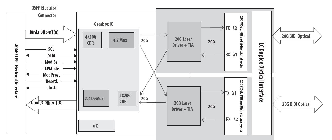
Transceiver Block Diagram
• Absolute Maximum Ratings
|
Parameter |
Symbol |
Min. |
Typical |
Max. |
Unit |
| Storage Temperature |
TS |
-40 |
|
+85 |
°C |
| Supply Voltage |
VCCT, R |
-0.5 |
|
4 |
V |
| Relative Humidity |
RH |
0 |
|
85 |
% |
• Recommended Operating Environment:
|
Parameter |
Symbol |
Min. |
Typical |
Max. |
Unit |
| Case operating Temperature |
TC |
0 |
|
+70 |
°C |
| Supply Voltage |
VCCT, R |
+3.13 |
3.3 |
+3.47 |
V |
| Supply Current |
ICC |
|
|
1000 |
mA |
| Power Dissipation |
PD |
|
|
3.5 |
W |
• Electrical Characteristics (TOP = 0 to 70 °C, VCC = 3.13 to 3.47 Volts
|
Parameter |
Symbol |
Min |
Typ |
Max |
Unit |
Note |
| Data Rate per Channel |
|
- |
10.3125 |
11.2 |
Gbps |
|
| Power Consumption |
|
- |
2.5 |
3.5 |
W |
|
| Supply Current |
Icc |
|
0.75 |
1.0 |
A |
|
| Control I/O Voltage-High |
VIH |
2.0 |
|
Vcc |
V |
|
| Control I/O Voltage-Low |
VIL |
0 |
|
0.7 |
V |
|
| Inter-Channel Skew |
TSK |
|
|
150 |
Ps |
|
| RESETL Duration |
|
|
10 |
|
Us |
|
| RESETL De-assert time |
|
|
|
100 |
ms |
|
| Power On Time |
|
|
|
100 |
ms |
|
| Transmitter | ||||||
| Single Ended Output Voltage Tolerance |
|
0.3 |
|
4 |
V |
1 |
| Common mode Voltage Tolerance |
|
15 |
|
|
mV |
|
| Transmit Input Diff Voltage |
VI |
120 |
|
1200 |
mV |
|
| Transmit Input Diff Impedance |
ZIN |
80 |
100 |
120 |
|
|
| Data Dependent Input Jitter |
DDJ |
|
|
0.1 |
UI |
|
| Data Input Total Jitter |
TJ |
|
|
0.28 |
UI |
|
| Receiver | ||||||
| Single Ended Output Voltage Tolerance |
|
0.3 |
|
4 |
V |
|
| Rx Output Diff Voltage |
Vo |
|
600 |
800 |
mV |
|
| Rx Output Rise and Fall Voltage |
Tr/Tf |
|
|
35 |
ps |
1 |
| Total Jitter |
TJ |
|
|
0.7 |
UI |
|
| Deterministic Jitter |
DJ |
|
|
0.42 |
UI |
|
Note:
- 20~80%
• Optical Parameters(TOP = 0 to 70 °C, VCC = 3.0 to 3.6 Volts)
|
Parameter |
Symbol |
Min |
Typ |
Max |
Unit |
Ref. |
| Transmitter | ||||||
| Optical Wavelength CH1 |
λ |
832 |
850 |
868 |
nm |
|
| Optical Wavelength CH2 |
λ |
882 |
900 |
918 |
nm |
|
| RMS Spectral Width |
Pm |
|
0.5 |
0.65 |
nm |
|
| Average Optical Power per Channel |
Pavg |
-4 |
-2.5 |
+5.0 |
dBm |
|
| Laser Off Power Per Channel |
Poff |
|
|
-30 |
dBm |
|
| Optical Extinction Ratio |
ER |
3.5 |
|
|
dB |
|
| Relative Intensity Noise |
Rin |
|
|
-128 |
dB/HZ |
1 |
| Optical Return Loss Tolerance |
|
|
|
12 |
dB |
|
| Receiver | ||||||
| Optical Center Wavelength CH1 |
λ |
882 |
900 |
918 |
nm |
|
| Optical Center Wavelength CH2 |
λ |
832 |
850 |
868 |
nm |
|
| Receiver Sensitivity per Channel |
R |
|
-11 |
|
dBm |
|
| Maximum Input Power |
PMAX |
+0.5 |
|
|
dBm |
|
| Receiver Reflectance |
Rrx |
|
|
-12 |
dB |
|
| LOS De-Assert |
LOSD |
|
|
-14 |
dBm |
|
| LOS Assert |
LOSA |
-30 |
|
|
dBm |
|
| LOS Hysteresis |
LOSH |
0.5 |
|
|
dB |
|
Note
- 12dB Reflection
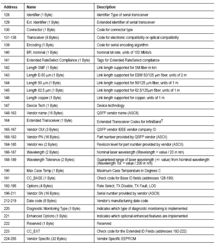
Page02 is User EEPROM and its format decided by user.
The detail description of low memory and page00.page03 upper memory please see SFF-8436 document.
• Timing for Soft Control and Status Functions
|
Parameter |
Symbol |
Max |
Unit |
Conditions |
| Initialization Time | t_init | 2000 | ms | Time from power on1, hot plug or rising edge of Reset until the module is fully functional2 |
| Reset Init Assert Time | t_reset_init | 2 | μs | A Reset is generated by a low level longer than the minimum reset pulse time present on the ResetL pin. |
| Serial Bus Hardware Ready Time | t_serial | 2000 | ms | Time from power on1 until module responds to data transmission over the 2-wire serial bus |
| Monitor Data ReadyTime | t_data | 2000 | ms | Time from power on1 to data not ready, bit 0 of Byte 2, deasserted and IntL asserted |
| Reset Assert Time | t_reset | 2000 | ms | Time from rising edge on the ResetL pin until the module is fully functional2 |
| LPMode Assert Time | ton_LPMode | 100 | μs | Time from assertion of LPMode (Vin:LPMode =Vih) until module power consumption enters lower Power Level |
| IntL Assert Time | ton_IntL | 200 | ms | Time from occurrence of condition triggering IntL until Vout:IntL = Vol |
| IntL Deassert Time | toff_IntL | 500 | μs | toff_IntL 500 μs Time from clear on read3 operation of associated flag until Vout:IntL = Voh. This includes deassert times for Rx LOS, Tx Fault and other flag bits. |
| Rx LOS Assert Time | ton_los | 100 | ms | Time from Rx LOS state to Rx LOS bit set and IntL asserted |
| Flag Assert Time | ton_flag | 200 | ms | Time from occurrence of condition triggering flag to associated flag bit set and IntL asserted |
| Mask Assert Time | ton_mask | 100 | ms | Time from mask bit set4 until associated IntL assertion is inhibited |
| Mask De-assert Time | toff_mask | 100 | ms | Time from mask bit cleared4 until associated IntlL operation resumes |
| ModSelL Assert Time | ton_ModSelL | 100 | μs | Time from assertion of ModSelL until module responds to data transmission over the 2-wire serial bus |
| ModSelL Deassert Time | toff_ModSelL | 100 | μs | Time from deassertion of ModSelL until the module does not respond to data transmission over the 2-wire serial bus |
| Power_over-ride orPower-set Assert Time | ton_Pdown | 100 | ms | Time from P_Down bit set 4 until module power consumption enters lower Power Level |
| Power_over-ride or Power-set De-assert Time | toff_Pdown | 300 | ms | Time from P_Down bit cleared4 until the module is fully functional3 |
Note:
1. Power on is defined as the instant when supply voltages reach and remain at or above the minimum specified value.
2. Fully functional is defined as IntL asserted due to data not ready bit, bit 0 byte 2 de-asserted.
3. Measured from falling clock edge after stop bit of read transaction.
4. Measured from falling clock edge after stop bit of write transaction.
• Pin Assignment
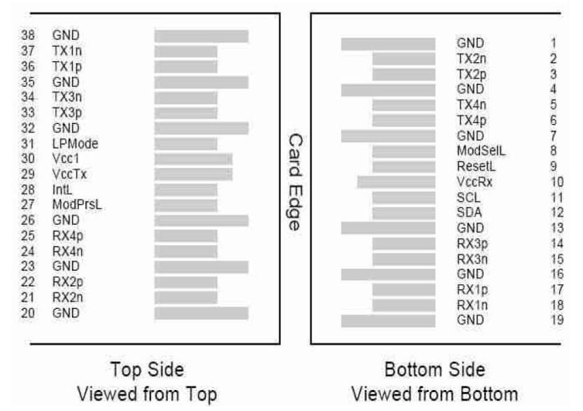
Diagram of Host Board Connector Block Pin Numbers and Name
• Pin Description
|
Pin |
Logic |
Symbol |
Name/Description |
Ref. |
|
1 |
|
GND |
Ground |
1 |
|
2 |
CML-I |
Tx2n |
Transmitter Inverted Data Input |
|
|
3 |
CML-I |
Tx2p |
Transmitter Non-Inverted Data output |
|
|
4 |
|
GND |
Ground |
1 |
|
5 |
CML-I |
Tx4n |
Transmitter Inverted Data Output |
|
|
6 |
CML-I |
Tx4p |
Transmitter Non-Inverted Data Output |
|
|
7 |
|
GND |
Ground |
1 |
|
8 |
LVTTL-I |
ModSelL |
Module Select |
|
|
9 |
LVTTL-I |
ResetL |
Module Reset |
|
|
10 |
|
VccRx |
+3.3V Power Supply Receiver |
2 |
|
11 |
LVCMOS-I/O |
SCL |
2-Wire Serial Interface Clock |
|
|
12 |
LVCMOS-I/O |
SDA |
2-Wire Serial Interface Data |
|
|
13 |
|
GND |
Ground |
1 |
|
14 |
CML-O |
Rx3p |
Receiver Inverted Data Output |
|
|
15 |
CML-O |
Rx3n |
Receiver Non-Inverted Data Output |
|
|
16 |
|
GND |
Ground |
1 |
|
17 |
CML-O |
Rx1p |
Receiver Inverted Data Output |
|
|
18 |
CML-O |
Rx1n |
Receiver Non-Inverted Data Output |
|
|
19 |
|
GND |
Ground |
1 |
|
20 |
|
GND |
Ground |
1 |
|
21 |
CML-O |
Rx2n |
Receiver Inverted Data Output |
|
|
22 |
CML-O |
Rx2p |
Receiver Non-Inverted Data Output |
|
|
23 |
|
GND |
Ground |
1 |
|
24 |
CML-O |
Rx4n |
Receiver Inverted Data Output |
|
|
25 |
CML-O |
Rx4p |
Receiver Non-Inverted Data Output |
|
|
26 |
|
GND |
Ground |
1 |
|
27 |
LVTTL-O |
ModPrsL |
Module Present |
|
|
28 |
LVTTL-O |
IntL |
Interrupt |
|
|
29 |
|
VccTx |
+3.3V Power Supply Transmitter |
2 |
|
30 |
|
Vcc1 |
+3.3V Power Supply |
2 |
|
31 |
LVTTL-I |
LPMode |
Low Power Mode |
|
|
32 |
|
GND |
Ground |
1 |
|
33 |
CML-I |
Tx3p |
Transmitter Inverted Data Output |
|
|
34 |
CML-I |
Tx3n |
Transmitter Non-Inverted Data Output |
|
|
35 |
|
GND |
Ground |
1 |
|
36 |
CML-I |
Tx1p |
Transmitter Inverted Data Output |
|
|
37 |
CML-I |
Tx1n |
Transmitter Non-Inverted Data Output |
|
|
38 |
|
GND |
Ground |
1 |
Notes:
- GND is the symbol for single and supply(power) common for QSFP modules, All are common within the QSFP module and all module voltages are referenced to this potential otherwise noted. Connect these directly to the host board signal common ground plane. Laser output disabled on TDIS >2.0V or open, enabled on TDIS <0.8V.
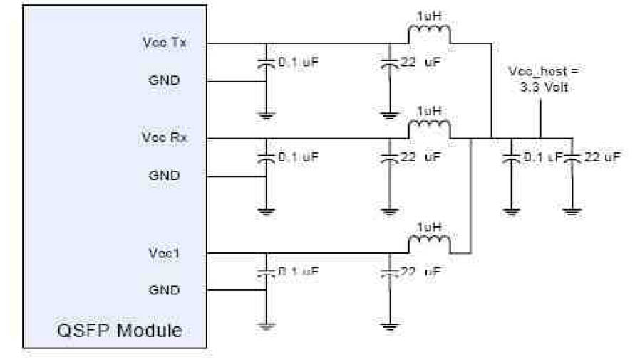
- VccRx, Vcc1 and VccTx are the receiver and transmitter power suppliers and shall be applied concurrently. Recommended host board power supply filtering is shown below. VccRx, Vcc1 and VccTx may be internally connected within the QSFP transceiver module in any combination. The connector pins are each rated for maximum current of 500mA.
• Recommended Circuit
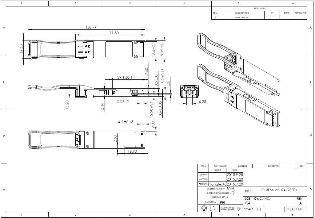
Mechanical Dimensions