
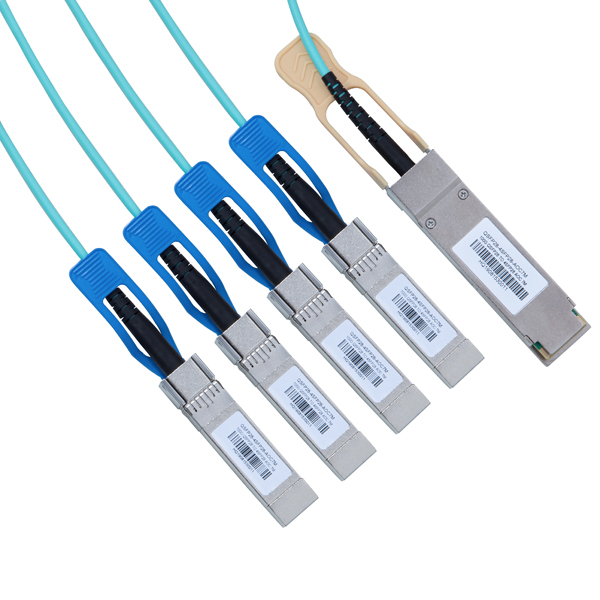
100-4*25G Active optical cabel (QSFP28-4*SFP28) JHA-QSFP28-4SFP28-100G-AOC


Features
◊ Support 4x25GBASE-SR application
◊ Compliant to QSFP28 MSA SFF-8636 and SFP28 MSA SFF-8431 and SFF- 8472
◊ Multi rate of up to 25.78125Gbps per lane
◊ Transmission distance up to 50m
◊ +3.3V single power supply
◊ Low power consumption
◊ UL certification cables (optional)
◊ Operating temp Commercial: 0°C to +70 °C
◊ RoHS compliant
Applications
◊ 4x25Gbe-SR
◊ Other optical links
Specification:
Absolute Maximum Ratings
Table1- Absolute Maximum Ratings
|
Parameter |
Symbol |
Min. |
Typical |
Max. |
Unit |
Notes |
|
Supply Voltage |
Vcc3 |
-0.5 |
- |
+3.6 |
V |
|
|
Storage Temperature |
Ts |
-10 |
- |
+70 |
°C |
|
|
Operating Humidity |
RH |
+5 |
- |
+85 |
% |
1 |
Note: 1 No condensation
Recommended Operating Conditions
Table 2- Recommended operating Conditions
| Parameter | Symbol | Min. | Typical |
Max. |
Unit | Notes |
| Operating Temperature | TC | 0 | - |
+70 |
°C | |
| Power Supply Voltage | Vcc | 3.14 | 3.3 |
3.47 |
V | |
| Power Dissipation per QSFP28 | Pd | - | - |
2.5 |
W | |
| Power Dissipation per SFP28 | Pd | - | - |
1.0 |
W | 1 |
| Bit Rate per Lane | BR | 10.3125 | 25.78125 | - | Gbps |
Note: 1 Per terminal
Electrical Characteristics
Table 3- Electrical Characteristics for QSFP28
| Parameter | Symbol | Min. | Typ. | Max. | Units | Notes | |
| ModSelL | Module Select | VOL | 0 | - | 0.8 | V | |
| Module Unselect | VOH | 2.5 | - | VCC | V | ||
| LPMode | Low Power Mode | VIL | 0 | - | 0.8 | V | |
| Normal Operation | VIH | 2.5 | - | VCC+0.3 | V | ||
| ResetL | Reset | VIL | 0 | - | 0.8 | V | |
| Normal Operation | VIH | 2.5 | - | VCC+0.3 | V | ||
| ModPrsL | Normal Operation | VOL | 0 | - | 0.4 | V | |
| IntL | Interrupt | VOL | 0 | - | 0.4 | V | |
| Normal Operation | VoH | 2.4 | - | VCC | V | ||
| Electrical Transmitter Characteristics | |||||||
| Differential Date Input Swing | Vin,P-P | 200 | - | 1600 | mV | ||
| Output Differential Impedance | ZIN | 90 | 100 | 110 | Ω | ||
| Electrical Receiver Characteristics | |||||||
| Differential Data Output Swing | Vout | 200 | - | 800 | mVPP | ||
| Bit Error Rate | BER | E-12 | 1 | ||||
| Input Differential Impedance | ZD | 90 | 100 | 110 | Ω | ||
Note: 1 PRBS2^31-1@25.78125Gbps
Table 4- Electrical Characteristics for SFP28
| Parameter | Symbol | Min. | Typ. |
Max. |
Units | Notes | ||||
| Electrical Transmitter Characteristics | ||||||||||
| Differential Data Input Swing | Vin,P-P | 200 | - | 1600 | mVPP | |||||
| Input Differential Impedance | ZIN | 90 | 100 | 110 | Ω | |||||
| Tx_Fault | Normal Operation | VOL | 0 | - | 0.8 | V | ||||
| Transmitter Fault | VOH | 2.0 | - | VCC | V | |||||
| Tx_Disable | Normal Operation | VIL | 0 | - | 0.8 | V | ||||
| Laser Disable | VIH | 2.0 | - | VCC+0.3 | V | |||||
| Electrical Receiver Characteristics | ||||||||||
| Differential Date Output | Vout | 400 | - |
800 |
mV | |||||
| Bit Error Rate | BER | - | - |
E-12 |
- | |||||
| Output Differential Impedance | ZD | 90 | 100 |
110 |
Ω | |||||
| Rx_LOS | Normal Operation | VOL | 0 | - |
0.8 |
V | ||||
| Lose Signal | VoH | 2.0 | - |
VCC |
V | |||||
Pin arrangement
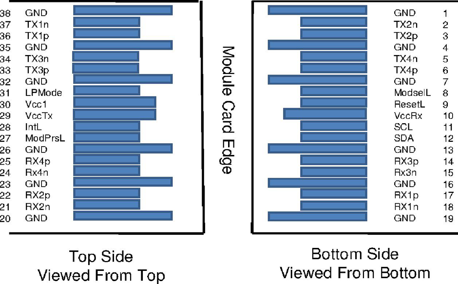
Figure 1, Pin View for QSFP28
Table 5- Pin Function Definitions for QSFP28
| Pin | Symbol | Name/Description | Notes |
| 1 | GND | Ground | 1 |
| 2 | Tx2n | Transmitter Inverted Data Input | |
| 3 | Tx2p | Transmitter Non-Inverted Data Input | |
| 4 | GND | Ground | 1 |
| 5 | Tx4n | Transmitter Inverted Data Input | |
| 6 | Tx4p | Transmitter Non-Inverted Data Input | |
| 7 | GND | Ground | 1 |
| 8 | ModSelL | Module Select | |
| 9 | ResetL | Module Reset | |
| 10 | Vcc Rx | +3.3V Power Supply Receiver | |
| 11 | SCL | 2-wire serial interface clock | |
| 12 | SDA | 2-wire serial interface data | |
| 13 | GND | Ground | 1 |
| 14 | Rx3p | Receiver Non-Inverted Data Output | |
| 15 | Rx3n | Receiver Inverted Data Output | |
| 16 | GND | Ground | 1 |
| 17 | Rx1p | Receiver Non-Inverted Data Output | |
| 18 | Rx1n | Receiver Inverted Data Output | |
| 19 | GND | Ground | 1 |
| 20 | GND | Ground | 1 |
| 21 | Rx2n | Receiver Inverted Data Output | |
| 22 | Rx2p | Receiver Non-Inverted Data Output | |
| 23 | GND | Ground | 1 |
| 24 | Rx4n | Receiver Inverted Data Output |
| Pin |
Symbol |
Name/Description | Notes |
| 25 | Rx4p | Receiver Non-Inverted Data Output | |
| 26 | GND | Ground | 1 |
| 27 |
ModPrsL |
Module Present | |
| 28 | IntL | Interrupt | |
| 29 | Vcc Tx | +3.3V Power supply transmitter | |
| 30 | Vcc1 | +3.3V Power supply | |
| 31 |
LPMode |
Low Power Mode | |
| 32 | GND | Ground | 1 |
| 33 | Tx3p | Transmitter Non-Inverted Data Input | |
| 34 | Tx3n | Transmitter Inverted Data Input | |
| 35 | GND | Ground | 1 |
| 36 | Tx1p | Transmitter Non-Inverted Data Input | |
| 37 | Tx1n | Transmitter Inverted Data Input | |
| 38 | GND | Ground | 1 |
Note: 1. Circuit ground is internally isolated from chassis ground.
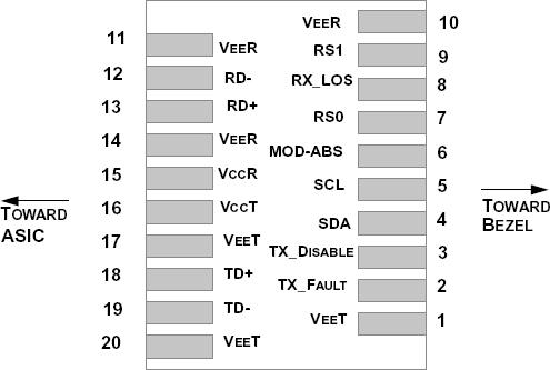
Figure 2, Pin View for SFP28
Table 6-Pin Function Definitions
| Pin | Symbol | Name/Description | Notes |
| 1 | VEET | Module Transmitter Ground | 1 |
| 2 | TX_FAULT | Module Transmitter Fault | 2 |
| 3 | TX_DISABLE | Transmitter Disable; Turns off transmitter laser output | 3 |
| 4 | SDA | 2-Wire Serial Interface Data Line (MOD-DEF2) | |
| 5 | SCL | 2-Wire Serial Interface Clock (MOD-DEF1) | |
| 6 | MOD_ABS | Module Absent, connected to VEET or VEER in the module | 2 |
| 7 | RS0 | Rate Select 0, optionally controls SFP+ module receiver | 4 |
| 8 | RX_LOS | Receiver Loss of Signal Indication (In FC designated as Rx_LOS and in Ethernet designated as NOT Signal Detect) | 2 |
| 9 | RS1 | Rate Select 1, optionally controls SFP+ module transmitter | 4 |
| Pin | Symbol | Name/Description | Notes |
| 10 | VEER | Module Receiver Ground | 1 |
| 11 | VEER | Module Receiver Ground | 1 |
| 12 | RD- | Receiver Inverted Data Output | |
| 13 | RD+ | Receiver Non-Inverted Data Output | |
| 14 | VEER | Module Receiver Ground | 1 |
| 15 | VCCR | Module Receiver 3.3 V Supply | |
| 16 | VCCT | Module Transmitter 3.3 V Supply | |
| 17 | VEET | Module Transmitter Ground | 1 |
| 18 | TD+ | Transmitter Non-Inverted Data Input | |
| 19 | TD- | Transmitter Inverted Data Input | |
| 20 | VEET | Module Transmitter Ground | 1 |
Note:
- The module ground pins are isolated from the module case.
- The pins shall be pulled up with 4.7K-10Kohms to a voltage between 3.14V and 3.46V on host board.
- The pin is pulled up to VCCT with a 4.7K-10KΩ resistor in the module.
- See SFF-8472 Rev12.2 Table 10-2.
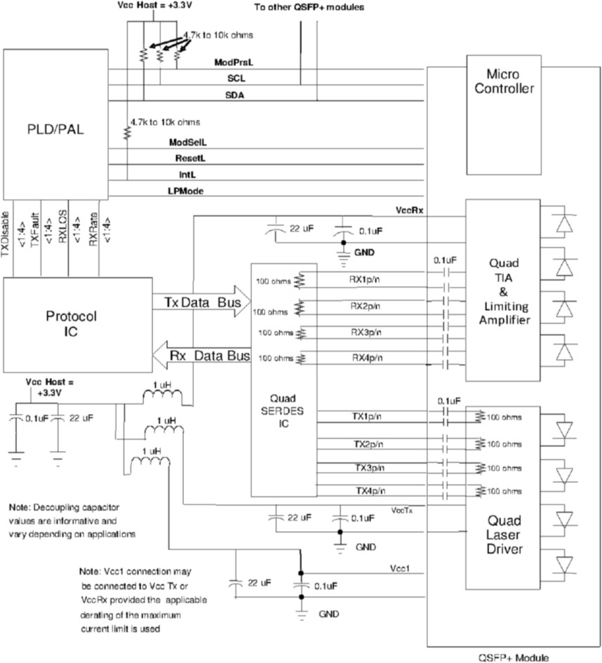
Recommended Circuit
Figure 3, Recommended Interface Circuit for QSFP28
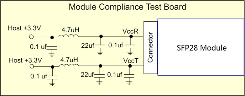
Figure 4, Recommended Host Board Power Supply Circuit for SFP28
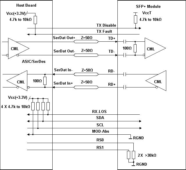
Figure 5, Recommended Interface Circuit for SFP28
Monitoring Specification
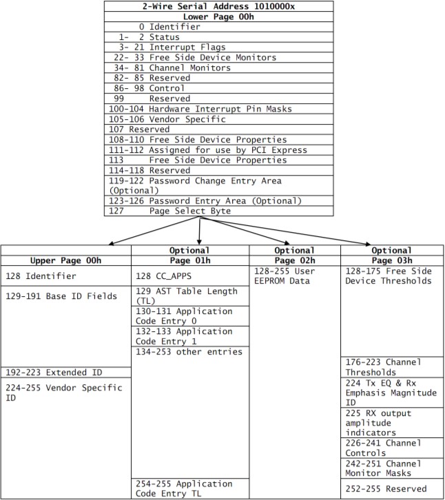
Figure 6, Memory Map for QSFP28

Figure 7, Memory Map for SFP28
Mechanical
Unit mm
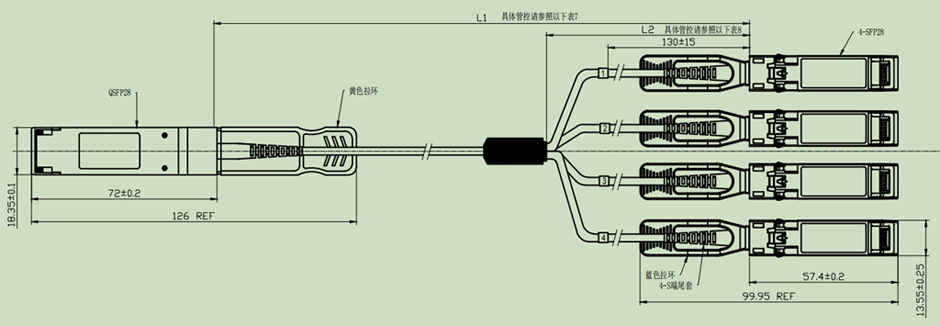
Figure 8, Mechanical Diagram
Table 7- Cable Length
| Cable Length L1(Unit: m) | Tolerant(Unit: cm) |
| ≤1.0 | +5/-0 |
| 1.0<L≤4.5 | +15/-0 |
| 4.5<L≤14.5 | +30/-0 |
| >14.5 | +2%/-0 |
Table 8- Breakout Cable Nominal Length
|
Total Length L1 (Unit: m) |
Breakout Point Measured from SFPL2(Unit: m) |
| 1 | 0.7 |
| 2 | 1.4 |
| 3 | 2 |
| ≥5 | 3 |
Warnings
Handling Precautions: This device is susceptible to damage as a result of electrostatic discharge (ESD).
A static free environment is highly recommended. Follow guidelines according to proper ESD procedures.
Laser Safety: Radiation emitted by laser devices can be dangerous to human eyes. Avoid eye exposure to direct or indirect radiation.


